16.3
Special Purpose Junction Diodes
Semiconductor Devices · Maharashtra HSC
Theory
The four devices
Four special purpose junction diodes are studied: the Zener diode, the photodiode, the solar cell, and the Light Emitting Diode (LED). The Zener diode works on the principle of junction breakdown; the other three make use of photosensitivity, an important and useful property of semiconductors.
16.3.1 Zener diode
Junction breakdown
When the reverse bias voltage of an ordinary junction diode is increased beyond a critical voltage, the reverse current increases sharply to a high value. That critical voltage is the reverse breakdown voltage, and an ordinary diode is damaged at this stage. Electrical breakdown of any material can occur by avalanche breakdown or by Zener breakdown; the syllabus discusses Zener breakdown.
Zener breakdown — mechanism
- When the reverse voltage across a p-n junction diode is increased, the electric field across the junction increases.
- This results in a force of attraction on the negatively charged electrons at the junction.
- The covalent bonds which hold the semiconductor together are broken by this force and electrons are removed from the bonds.
- These free electrons are then available for electrical conduction and result in a large current.
- As the applied voltage is increased further, the field increases and more and more electrons are removed from their covalent bonds, so the net current increases rapidly with the applied voltage.
- Zener breakdown occurs in diodes which are heavily doped, so that the depletion layer is narrow. Zener breakdown does not damage the diode. The field strength at breakdown in such a diode is about .
Definition and symbol
A Zener diode is a heavily doped p-n junction diode designed to work in the breakdown region. Because of the heavy doping, it has a very thin depletion layer. It is used as a voltage regulator or voltage stabiliser.
Symbol in words: the ordinary diode symbol — a solid triangle pointing towards a straight bar — with the bar bent forward at the top and backward at the bottom, so that the cathode line looks like the letter Z.
I-V characteristic, described in words
- Forward bias (first quadrant): the Zener diode behaves exactly like a normal diode. Almost no current until the knee voltage, then the current rises steeply.
- Reverse bias (third quadrant): only a very small reverse saturation current flows as the reverse voltage is increased, until the reverse voltage reaches the Zener voltage . At the reverse current suddenly increases and the curve drops almost vertically downwards.
- The important feature: once breakdown has occurred, the voltage across the diode remains constant at even though the current through it increases by a large amount. This constant-voltage property is what is used in a voltage regulator.
- depends on the amount of doping. A heavily doped diode has a thin depletion layer and breaks down at a lower reverse voltage; a lightly doped diode has a higher breakdown voltage. Zener diodes with breakdown voltage less than operate mainly in the Zener breakdown region, those greater than operate mainly in the avalanche breakdown region, but both are called Zener diodes.
Zener diode as a voltage regulator
A voltage regulator maintains a constant voltage across a load regardless of variations in the applied input voltage and variations in the load current.
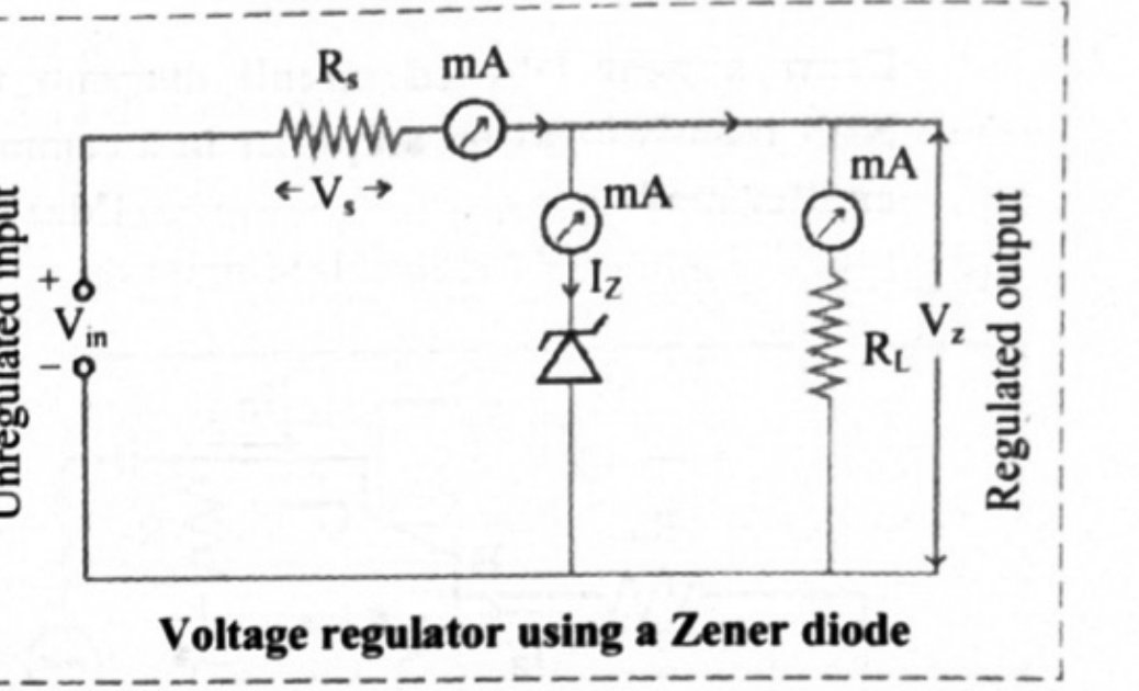
Circuit in words: a series resistance is connected from the positive terminal of the unregulated input supply to the cathode of the Zener diode. The Zener diode is connected in reverse bias, cathode to the positive side, with its anode returning to the negative terminal of the supply. The load resistance is connected in parallel with the Zener diode. The regulated output is taken across . The requirement is , and limits the current flowing through the diode. Because is in parallel with the Zener, the voltage across is always equal to the Zener voltage, .
Working — the board's own sequence:
- When a Zener diode is operated in the breakdown region (reverse bias), the voltage across it remains almost constant even if the current through it changes by a large amount. Hence it can be used as a voltage regulator.
- A Zener diode of breakdown voltage is connected in reverse bias to an input voltage source , with .
- If the input voltage increases, the current through and the Zener diode also increases. This results in an increase in the voltage across the resistance , but the voltage across the Zener diode does not change.
- The series resistance absorbs the output voltage fluctuations and maintains a constant voltage across the load resistance. Hence the output voltage remains constant irrespective of the change in the input voltage.
- If the input voltage is constant but the load resistance decreases, the load current increases. This extra current cannot come from the source, because the drop across does not change while the Zener is within its regulating range. The increase in is compensated by a decrease in the Zener current , keeping constant.
- The voltage across the Zener diode remains constant at its breakdown voltage for all values of Zener current , as long as the current stays in the breakdown region.
- Hence a regulated DC output voltage is obtained across whenever the input voltage remains within a minimum and a maximum value.
Choosing the series resistance
When there is no load ( infinite), the load current is zero and all the circuit current passes through the Zener diode, giving maximum power dissipation in the diode. Similarly a small value of gives a large diode current when a large is connected. The value of is therefore chosen so that the maximum power rating of the Zener diode is not exceeded when there is no load or the load is very high. The maximum power rating is
Voltage stabilisation is effective only when there is a minimum Zener current, and the supply voltage must always be greater than .
Specifications on a Zener diode datasheet
- Zener V-I characteristic.
- Zener voltage , also called the reverse voltage — the voltage at which the diode breaks down in reverse bias, and at which it is operated.
- Maximum Zener current or — the maximum current that can flow through the diode at its rated voltage .
- Power rating — the maximum power that can be dissipated by the Zener diode package.
- Zener resistance , also called Zener impedance — the opposition offered to the current in the operating region. It behaves like a small resistance in series with the ideal Zener, so changes in cause small changes in ; this is why is not strictly constant.
Applications of a Zener diode
Voltage regulator; fixed reference voltage provider in transistor biasing circuits; peak clipper or limiter in wave shaping circuits; protection of a meter against damage from accidental fluctuations.
Worked example (Example 16.2)
A stabilised supply is to be designed from a DC source using a Zener of maximum power rating .
- Maximum Zener current: .
- Minimum series resistance: .
- Load current with : .
- Zener current at full load: .
16.3.2 Photodiode
Definition and symbol
A photodiode is a special type of p-n junction diode which converts light energy into electrical energy. It generates current when exposed to light and is also called a photodetector or photosensor. It operates in reverse biased mode, and only minority carrier current flows through it.
Symbol in words: the ordinary diode symbol with two small arrows pointing towards the junction, showing light falling on it. The triangle side is the anode, the bar side the cathode.
Construction
The p-n junction of a photodiode is placed inside a glass material so that only the junction is exposed to light. The other part of the diode is painted with an opaque colour or covered, so that stray light cannot reach it.
Working principle — the board's own sequence
- When a p-n junction diode is reverse biased, a reverse saturation current flows through the junction.
- The magnitude of this current is constant for a certain range of reverse bias voltages. This current is due to the minority carriers on either side of the junction — electrons are the minority carriers in the p-region and holes are the minority carriers in the n-region.
- The reverse current depends only on the concentration of the minority carriers and not on the applied voltage. This current is called the dark current, because it flows even when the photodiode is not illuminated.
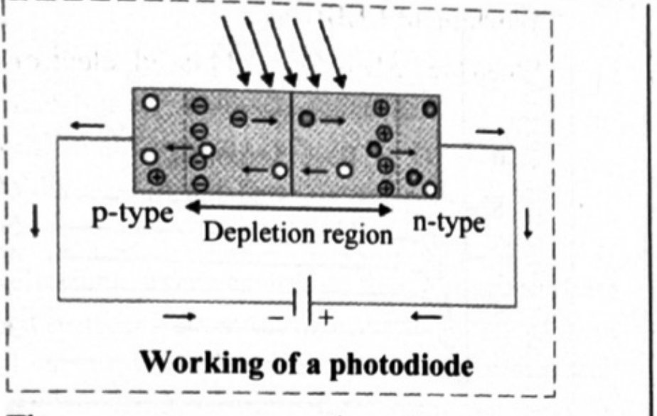
- When the p-n junction is illuminated with photons whose energy is greater than the band gap of the semiconductor, electron-hole pairs are generated in the depletion region.
- The electrons and the holes are separated due to the intrinsic electric field present in the depletion region. The electrons are attracted towards the anode and the holes towards the cathode. More carriers are therefore available for conduction and the reverse current increases.
- The reverse current of a photodiode depends on the intensity of the incident light. Thus the reverse current can be controlled by controlling the concentration of the minority carriers in the junction.
The total current through a photodiode is the sum of the photocurrent and the dark current.
Characteristics, described in words
- I-V characteristic: drawn in the reverse-bias region. For each fixed intensity of illumination the curve is nearly horizontal — the reverse current is almost independent of the reverse voltage. The curves are stacked one above another, the curve for a higher illumination lying at a higher reverse current. The bottom curve, for zero illumination, is the dark current.
- Reverse current versus intensity: a graph that rises with increasing intensity of illumination and then levels off at a constant value. That constant value is called the saturation current of the photodiode.
Dark resistance
Dark resistance is the resistance of a photodiode when it is not illuminated, defined as
The sensitivity of the device is increased by minimising the dark current.
Advantages, disadvantages, applications
- Advantages: quick response when exposed to light; linear response, the reverse current being linearly proportional to the intensity of the incident light; high speed of operation; light weight and compact size; wide spectral response (silicon photodiodes respond from in the UV to in the IR); relatively low cost.
- Disadvantages: properties are temperature dependent, like those of many semiconductor devices; low reverse current at low illumination levels.
- Applications: counters and switches; burglar alarm systems; detection of visible and invisible radiations; circuits requiring fast switching and high speed operation; fibre optic communication systems; optocouplers, which provide electrical isolation between two circuits; photo sensors or detectors for accurate measurement of light intensity; safety electronics such as fire and smoke detectors. The idea common to all of them is that a photodiode conducts whenever light strikes it and stops conducting the moment the light stops.
16.3.3 Solar cell (photovoltaic cell)
Principle
Solar energy is pollution free and available free of cost. Devices converting it into usable form are of two kinds: photothermal devices, which convert solar energy into heat, and photovoltaic devices, which convert solar energy into electrical energy using solar cells. Light incident on a solar cell produces both a current and a voltage, generating electric power; a solar cell thus works as a source of DC power. As the board puts it: a solar cell uses solar energy and converts it into electric energy, which is why it is also called a photovoltaic cell.
Structure
- It consists of a p-n junction.
- The n-side of the junction faces the solar radiation and is made thin, so that the incident light reaches the depletion region where the electron-hole pairs are generated.
- The p-side is relatively thick and is at the back of the cell.
- Both the p-side and the n-side are coated with a conducting material. The contact on the n-side is the front contact, and that on the p-side is the back or rear contact.
- The n-side carries an antireflection coating which allows visible light to pass through but reflects the IR (heat) radiation, protecting the cell from heat. This matters because the electronic properties of semiconductors are sensitive to temperature fluctuations. This coating also works as the electrical contact of the cell.
Material requirements: firstly it must be a photosensitive material which absorbs light and raises electrons to a higher energy state; secondly the higher energy electrons so generated must be able to be taken out of the cell into an external circuit, where they dissipate their energy and return to the cell.
Working — the four steps
- Electron-hole pairs are generated in the depletion region of the p-n junction. These are the photo-generated carriers.
- The electrons and holes are separated and collected at the cathode and the anode respectively.
- The carriers accumulate and generate a voltage across the solar cell.
- The power thus produced is dissipated (utilised) in the load resistance or the circuit connected across the cell.
The current produced is called the light-generated or photo-generated current, and it is a two-step process. First, incident photons of energy greater than the band gap are absorbed and generate electron-hole pairs. Normally such pairs would simply recombine and be lost, giving no current. In a solar cell they are spatially separated and prevented from recombining, by the intrinsic electric field of the depletion region: a light-generated electron in the p-type region that reaches the junction is swept across by the junction field into the n-type region, where it is now a majority carrier, and a light-generated hole similarly reaches the p-type region. Negative and positive charge therefore accumulate on the n-region and the p-region, and the cell acts as a voltage source. When an external circuit is connected, the light-generated carriers flow through it.
V-I characteristic, described in words
The illuminated characteristic is drawn in the fourth quadrant, because a solar cell supplies current to the load instead of drawing current from a source.
- The intersection of the curve with the current axis is the short circuit current , for the given light intensity. Here the load is short-circuited, the voltage is zero, and the power delivered is zero.
- The intersection of the curve with the voltage axis is the open circuit voltage , for the given light intensity. Here the load is open, the current is zero, and the power delivered is again zero.
- Between these two extremes there is one point on the curve at which the power delivered to the load is maximum — the maximum power point.
Criteria for selection of the material
- Band gap should be between and .
- It should have high optical absorption.
- It should have good electrical conductivity.
- The material should be easily available.
Most solar cell materials have a band gap of about : Si (), GaAs (), CdTe (), CuInSe (). Cells for domestic and space use are mostly silicon based. Solar cells are non-polluting, need little maintenance and last long, but have a high installation cost and low efficiency.
Uses of a solar cell
- Charging batteries during the day so that the batteries can supply power at night.
- Supplying power at remote places, to equipment ranging from calculators to satellites and space stations.
- Supplying power to traffic signals and to communication stations.
- In a lux meter, to measure the intensity of light.
16.3.4 Light Emitting Diode (LED)
Definition and symbol
The Light Emitting Diode, or LED, is a diode which emits light when a large forward current passes through it.
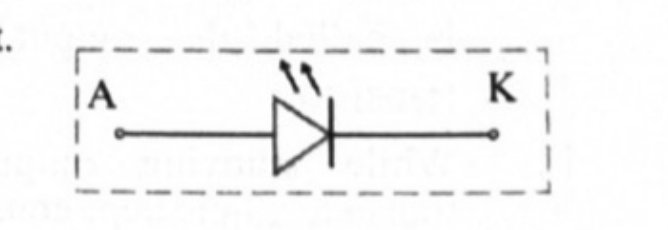
Symbol in words: the ordinary diode symbol — triangle pointing to a bar, anode A on the triangle side, cathode K on the bar side — with two small arrows drawn pointing away from the junction, indicating the emitted light.
Construction
- The n-region is more heavily doped than the p-region of the p-n junction.
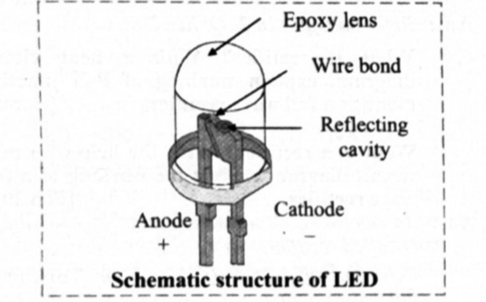
- The LED p-n junction is encased in a dome-shaped transparent case, so that light is emitted uniformly in all directions and internal reflections are minimised. The domed epoxy top acts like a lens and concentrates the light, which is why an LED looks brightest at the top.
- Metal electrodes attached on either side of the p-n junction serve as contacts for external electrical connection. The larger (longer) leg of an LED is the positive electrode or anode.
- The LED is fabricated in such a way that the light emitted is not reabsorbed into the material.
- It is ensured that the electron-hole recombination takes place at the surface, for maximum light output.
Working
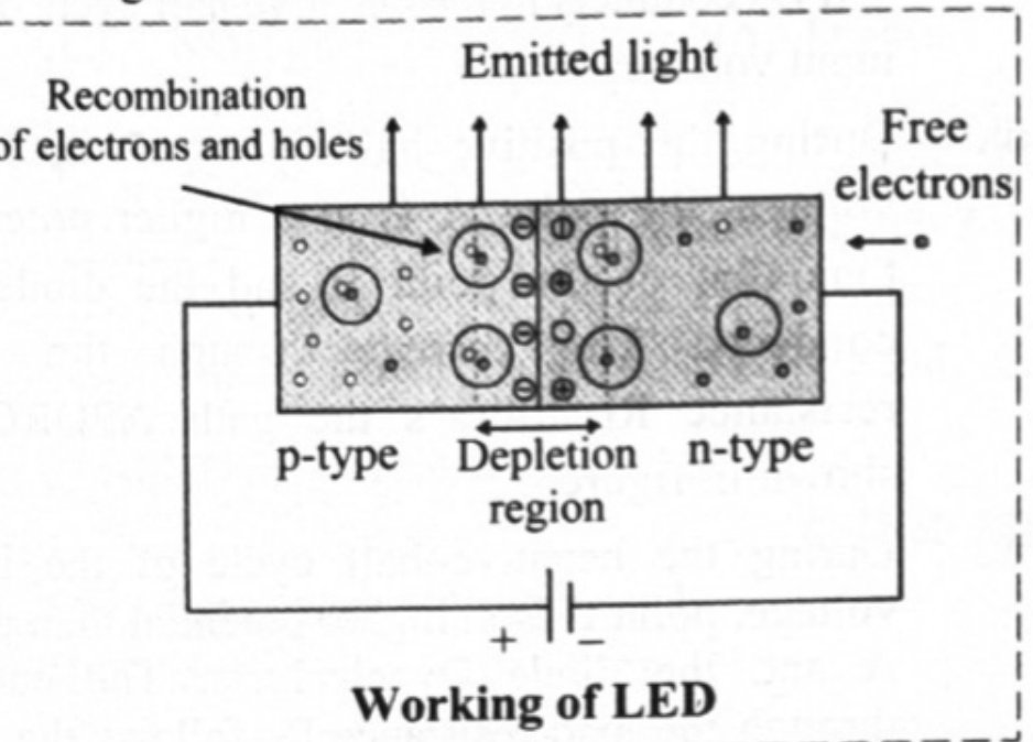
- When the LED is forward biased, electrons from the semiconductor's conduction band recombine with holes from the valence band, releasing sufficient energy to produce photons, which emit monochromatic (single colour) light.
- Because the layer is thin, a reasonable number of these photons can leave the junction and emit coloured light.
- The amount of light output is directly proportional to the forward current: the higher the forward current, the higher the light output.
I-V characteristic, described in words
The characteristic is similar to the forward characteristic of an ordinary diode: negligible current until the cut-in voltage is reached, after which the current rises steeply. The LED starts conducting after its cut-in voltage is reached. The forward voltage drop of an LED is much larger than that of an ordinary diode, around to . The current rating is only a few tens of milliampere, so a high resistance must be connected in series with an LED.
Colour and material
LEDs are fabricated using compound semiconductors made with elements such as gallium, phosphorus and arsenic. Varying the proportions changes the wavelength of the emitted light: AlGaAs gives infrared radiation, GaAsP gives red or yellow light, AlGaP gives red or green light, and ZnSe gives blue light. So the wavelength of the light emitted by an LED depends on the compound semiconductor used and the proportions of its constituent elements — that is, on the band gap of the material.
Advantages
Energy efficient (more light output per watt; up to lumens/watt); long lifetime ( hours or more); rugged, being solid state lights with no filament, tube or bulb to break; almost no warm-up period, emitting light within nanoseconds; excellent colour rendering, with colours that do not fade out; environment friendly, containing no mercury or other hazardous substances; controllable brightness and colour.
Disadvantages
Hazardous blue light quality, temperature dependence, voltage sensitivity, high initial cost.
Applications
Burglar alarm systems, counters, optical communication, indicator lamps in electrical equipment, display screens of cell phone handsets, LED television, vehicle head lamps, domestic and decorative illumination, street lighting, and seven segment displays used in calculators, electronic balances, watches and digital instruments.
White LED
White LEDs are made by wavelength conversion — partly or completely converting the radiation of an LED into white light. The least expensive method uses a blue LED to excite a yellow phosphor; the resulting mixture of blue and yellow light appears white. The blue LED was invented by Shuji Nakamura, who received the Nobel Prize in Physics in 2014.
Distinctions the board asks for
| Point | Zener diode | Ordinary diode |
|---|---|---|
| Doping | Heavily doped | Lightly doped |
| Depletion layer | Very thin | Comparatively wide |
| Operating region | Reverse breakdown region | Forward bias region |
| Effect of breakdown | Not damaged; recovers | Damaged permanently |
| Use | Voltage regulator or stabiliser | Rectifier, switch |
| Point | Photodiode | Solar cell |
|---|---|---|
| Bias | Always reverse biased | Needs no external bias; it is a source |
| Energy conversion | Light into a measurable electrical signal | Light into electrical power |
| Quadrant of characteristic | Reverse-bias (third) quadrant | Fourth quadrant |
| Junction area | Small | Large |
| Typical use | Detection and measurement of light | Generation of DC power |
Standard results
- ; ; ; ; .
- Zener field strength at breakdown, heavily doped diode: about ; is Zener breakdown, is avalanche breakdown.
- maximum reverse voltage divided by dark current; total photodiode current photocurrent dark current.
- Solar cell band gap window to ; Si , GaAs , CdTe , CuInSe .
- LED forward drop to ; current rating a few tens of milliampere; light output proportional to forward current.
Theory Questions Asked on This Subtopic
Real board questions. Answers are at the end of the page.
- 1
State the principle and uses of solar cell.
Maharashtra HSC board question — asked in March 2009Answer 1 ↓ - 2
Describe construction and working of light emitting diode (L.E.D.). State its 'any two' uses.
 Maharashtra HSC board question — asked in March 2010Answer 2 ↓
 - 3
With the help of a neat circuit diagram, explain the working of a photodiode. State its any 'two' uses.
 Maharashtra HSC board question — asked in October 2015Answer 3 ↓
 - 4
What is zener diode? How is it used as a voltage regulator?
 Maharashtra HSC board question — asked in March 2018Answer 4 ↓
 - 5
What is a Light Emitting Diode? Draw its circuit symbol.
 Maharashtra HSC board question — asked in February 2024Answer 5 ↓
Answers & Solutions
Work the questions above first, then check yourself here. Each answer is set out the way it should be written in the paper.
Solar cell uses solar energy and converts it into electric energy. Hence, it is also called as a photovoltaic cell. Uses of solar cell: i. Solar cells are used for charging batteries during day time so that batteries can supply power during night. ii. They are useful at remote places, for supplying power to various electronic equipments from calculators to satellites and space stations. iii. They are used to supply power to traffic signals, in communication stations, and in lux meter to measure intensity of light.
Construction of LED: In an LED, the n-region is heavily doped than the p-region of the p-n junction. ii. The LED p-n junction is encased in a dome-shaped transparent case so that light is emitted uniformly in all directions and internal reflections are minimized. iii. Metal electrodes attached on either side of the p-n junction serve as contacts for external electrical connection. The larger leg of a LED is the positive electrode or anode. iv. LED is fabricated in such a way that light emitted is not reabsorbed into the material. v. It is ensured that the electron-hole recombination takes place on the surface for maximum light output. Working of LED: i. When the LED is forward biased, electrons from the semiconductor's conduction band recombine with holes from the valence band releasing sufficient energy to produce photons which emit a monochromatic light. ii. Because of the thin layer, a reasonable number of these photons can leave the junction and emit coloured light. iii. The amount of light output is directly proportional to the forward current. Thus, higher the forward current, higher is the light output. iv. The given figure schematically shows the emission of light when electron-hole pair combines. Uses of LED: An LED is used in a variety of ways such as, i. burglar alarm system ii. counters iii. optical communication iv. indicator lamps in electric equipment v. display screen of a cell phone handset vi. LED television vii. vehicle head lamps viii. domestic and decorative illumination ix. street lighting. [Any two uses]
Working principle of photodiode: i. When a p-n junction diode is reverse biased, a reverse saturation current flows through the junction. ii. The magnitude of this current is constant for a certain range of reverse bias voltages. This current is due to the minority carriers on either side of the junction. The figure shows a schematic representation of working of a photodiode. iii. The reverse current depends only on the concentration of the minority carriers and not on the applied voltage. This reverse current is called dark current because it flows even when the photodiode is not illuminated. iv. When the p-n junction is illuminated with photons of energy greater than the band gap energy of semiconductor electron-hole pairs are generated in the depletion region. v. The electrons and the holes are separated due to the intrinsic electric field present in the depletion region. The electrons are attracted towards the anode and the holes are attracted towards the cathode. More carriers are available for conduction and the reverse current is increased. vi. The reverse current of a photodiode depends on the intensity of the incident light. Thus, the reverse current can be controlled by controlling the concentration of the minority carriers in the junction. Uses of photodiode: i. Counters and switches. ii. Burglar alarm systems. iii. Detection of visible and invisible radiations. iv. Circuits in which fast switching and high speed operations are required. v. Fibre optic communication systems. vi. Optocouplers, used to provide an electric isolation between two electronic circuits. vii. Photo sensors/detectors, for accurate measurement of light intensity. viii. Safety electronics like fire and smoke detectors. [Any two uses]
Zener diode: Zener diode is a heavily doped p-n junction diode. It has very thin depletion layer because of its heavy doping. Working of a Zener regulator: i. When a Zener diode is operated in the breakdown region (reverse bias), voltage across it remains almost constant even if the current through it changes by a large amount. Hence, it is used as a voltage regulator. ii. The given figure shows a circuit diagram of a voltage regulator using a Zener diode. iii. A Zener diode of break down voltage is connected in reverse bias to an input voltage source () as shown in figure. iv. If the input voltage increases, the current through and the Zener diode also increases. This results in an increase in the voltage across the resistance , but the voltage across the Zener diode does not change. v. The series resistance absorbs the output voltage fluctuations and maintains a constant voltage across the load resistance. vi. If the input voltage is constant, then the current and voltage drop across the series resistance remains same as the Zener is within its regulating range. In that case, if the load resistance () decreases then the load current () increases and this increase in is compensated by decrease in Zener current () keeping the Zener voltage () constant. vii. The voltage across the Zener diode remains constant at its break down voltage for all the values of Zener current as long as the current persists in the break down region. viii. Hence, a regulated DC output voltage is obtained across whenever the input voltage remains within a minimum and a maximum voltage.
Light Emitting Diode (LED): The Light Emitting Diode or LED is a diode which emits light when large forward current passes through it. Symbol: