16.4
Bipolar Junction Transistor (BJT)
Semiconductor Devices · Maharashtra HSC
Theory
What a BJT is
A junction transistor is a semiconductor device having two junctions and three terminals. The current in it is carried by both electrons and holes, which is why it is called a bipolar junction transistor. It has three doped regions forming a structure with two back to back p-n junctions.
Two types exist:
- n-p-n transistor: a p-type semiconductor (base) layer separates two layers of n-type semiconductor (emitter and collector). It is made by growing a thin layer of p-type semiconductor between two relatively thick layers of n-type semiconductor.
- p-n-p transistor: an n-type semiconductor (base) layer separates two layers of p-type semiconductor (emitter and collector), made by growing a thin n-type layer between two relatively thick p-type layers.
Symbols, described in words
Both symbols show a vertical bar (the base region) with the base lead coming in horizontally from the left, and two slanting leads leaving the bar on the right — the emitter (lower) and the collector (upper). The emitter lead carries an arrow, and the arrow shows the direction of the conventional current.
- n-p-n: the arrow points away from the base, i.e. outwards along the emitter lead.
- p-n-p: the arrow points from the emitter towards the base, i.e. inwards.
The three regions
| Region | Thickness and area | Doping | Function |
|---|---|---|---|
| Emitter (E) | Thick | Heavily doped | Supplies a large number of majority carriers for the current through the transistor |
| Base (B) | Thin, central layer | Lightly doped compared with the emitter | Lets most injected carriers pass through to the collector; controls the transistor action |
| Collector (C) | Area larger than that of the emitter and base | Intermediate — doped between emitter and base | Collects the major portion of the majority carriers supplied by the emitter; also helps dissipate heat |
Why the base is thin and lightly doped: if it were thick or heavily doped, most of the carriers injected from the emitter would recombine with the majority carriers in the base and form base current instead of reaching the collector. A thin, lightly doped base lets about of the emitter carriers diffuse across into the collector, leaving only about as base current — this is what makes transistor action possible.
Why the three regions are doped differently: heavy emitter doping provides plenty of carriers; light base doping and small base thickness minimise recombination in the base; intermediate collector doping with a large area allows the collector to collect nearly all the carriers and to dissipate the heat generated.
Depletion regions, currents, resistances
- Depletion regions are formed at the emitter-base junction and at the base-collector junction.
- The three currents are the emitter current , the base current and the collector current .
- The emitter-base junction has low resistance while the base-collector junction has high resistance.
Two-diode analogy
A transistor can be thought of as two junction diodes connected back to back — for an n-p-n, two diodes with their p-sides (anodes) joined at the base; for a p-n-p, two diodes with their n-sides (cathodes) joined at the base. This is only an analogy for remembering the structure; a real transistor cannot be made by wiring two diodes together, because the base must be thin enough for carriers to cross it.
Biasing
There are two p-n junctions in a transistor, the emitter-base (E-B) junction and the collector-base (C-B) junction, and they can be biased in different ways. In the most common method of biasing, used when the transistor is to work as an amplifier, the emitter-base junction is forward biased and the collector-base junction is reverse biased. This helps the easy flow of the majority carriers supplied by the emitter through the transistor.
Working of an n-p-n transistor
- Electrons are the majority carriers in the emitter of an n-p-n transistor, so the emitter current is due to electrons.
- The current through the E-B junction is large because that junction is forward biased. The current through the B-C junction is also large although that junction is reverse biased — the point of the whole explanation is why.
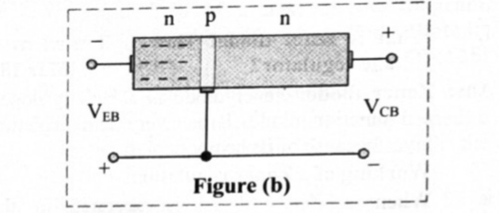
- At the instant the forward bias is applied to the E-B junction, the electrons in the emitter region have not yet entered the base region.
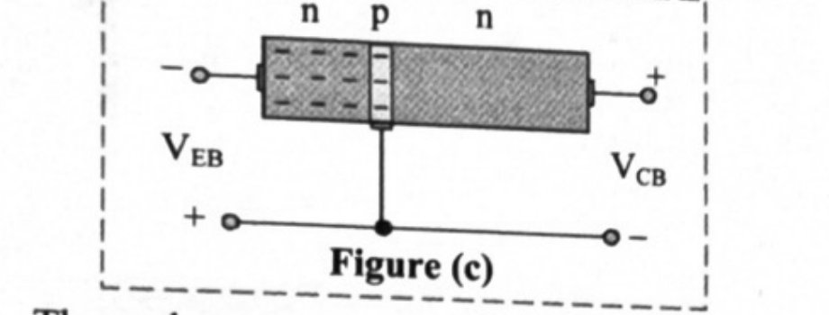
- When the biasing voltage becomes greater than the barrier potential ( to for the commonly used silicon transistors), many electrons enter the base region and form the emitter current .
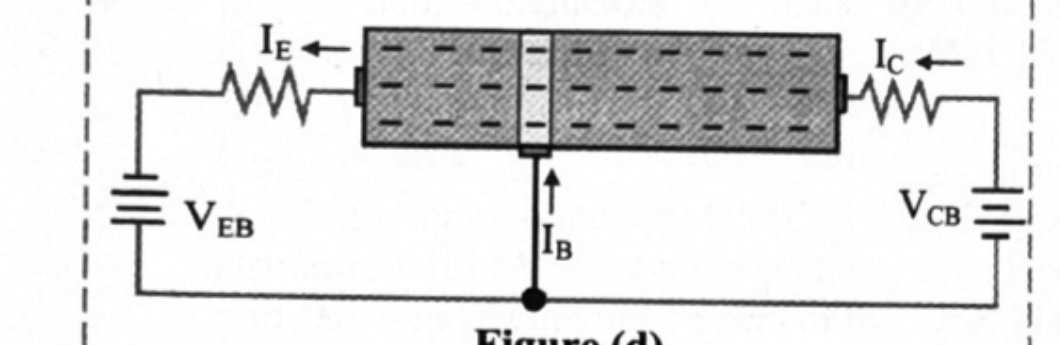
- These electrons can flow in two directions. They can flow through the base circuit and constitute the base current , or they can flow through the collector circuit and contribute to the collector current .
- The base current is small — about of — because the base is thin and lightly doped compared with the emitter.
- Electrons injected from the emitter into the base diffuse into the collector-base depletion region because the base region is thin. When they enter that depletion region they are pushed into the collector region by the electric field there. The collector current then flows through the external circuit. is about of .
- A p-n-p transistor works in exactly the same way, except that the majority carriers are now holes.
From this working,
and since is very small, .
Transistor configurations
The three possible configurations of a transistor in a circuit are common emitter (CE), where the emitter is common to both input and output; common base (CB), where the base is common to both; and common collector (CC), where the collector is common to both.
16.4.1 The Common Emitter (CE) configuration
The CE configuration is studied in detail because it is the most commonly used. In the common emitter, or grounded emitter, configuration the input signal is applied between the base and the emitter, and the output is obtained between the collector and the emitter.
Since the electrical relationship between , and is fixed by the physical construction of the transistor, any small change in the base current produces a much larger change in the collector current . A small current in the base thus controls the current in the emitter-collector circuit. Typical values of lie between and for general purpose transistors; if a transistor has , then one electron flows from the base terminal for every electrons flowing between the emitter and collector terminals.
The CE amplifier produces the highest current gain and power gain of all three configurations, mainly because the input impedance is low (the input is a forward biased p-n junction) while the output impedance is high (the output is taken from a reverse biased p-n junction).
The current gains
Since the current flowing out of the transistor must equal the current flowing in,
The current gain, called the current amplification factor, is defined as
and the ratio of the collector current to the emitter current is defined as
Combining these,
Relation between and — the derivation the board wants
Start from and divide throughout by :
16.4.2 The CE characteristics
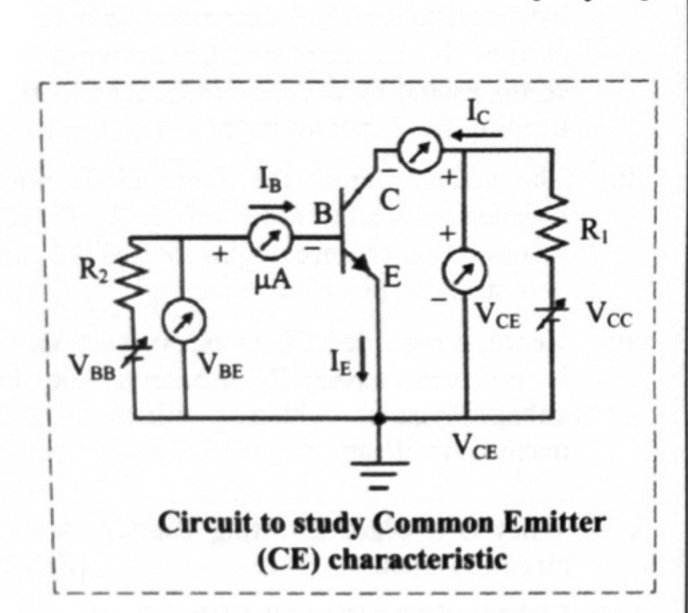
Circuit in words: an n-p-n transistor with its emitter earthed. In the input (base) circuit, a variable DC supply drives the base through a resistance, with a voltmeter reading across the base-emitter and a microammeter reading in the base lead. In the output (collector) circuit, a second variable DC supply drives the collector through the load resistance , with a voltmeter reading across the collector-emitter and a milliammeter reading in the collector lead. The input is applied as between base and emitter and the output is taken between collector and emitter.
Input characteristic
The variation of the base current with the base-emitter voltage is called the input characteristic. While studying the dependence of on , the collector-emitter voltage is kept fixed.
Described in words: the curve starts at the origin and stays almost flat along the axis — the current is very small until the barrier potential is overcome. Beyond the barrier potential the curve turns sharply upwards and rises rapidly with , exactly like the characteristic of a forward biased diode.
The input dynamic resistance of a transistor is the ratio of the change in the base-emitter voltage to the resulting change in the base current, at constant collector-emitter voltage:
Output characteristic
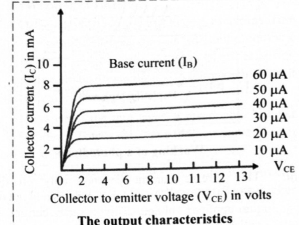
The variation of the collector current with the collector-emitter voltage is called the output characteristic of a transistor. The base current is kept constant while this is done.
Described in words: for each fixed value of a separate curve is drawn. Each curve rises very steeply from the origin for small and then flattens out, running almost parallel to the axis. The board's two statements about this graph are: the collector current is independent of as long as the collector-emitter junction is reverse biased, and the collector current is large for large values of the base current when is constant. So the family of curves rises in steps, one above another, as is increased.
The output dynamic resistance of a transistor is the ratio of the change in the collector-emitter voltage to the change in the collector current, at constant base current:
Because the flat part of the curve has a very small slope, is large.
16.4.3 Transistor as an amplifier
An amplifier is a device used for increasing the amplitude of an alternating signal (voltage, current or power). The standard circuit is an n-p-n transistor in common emitter configuration.
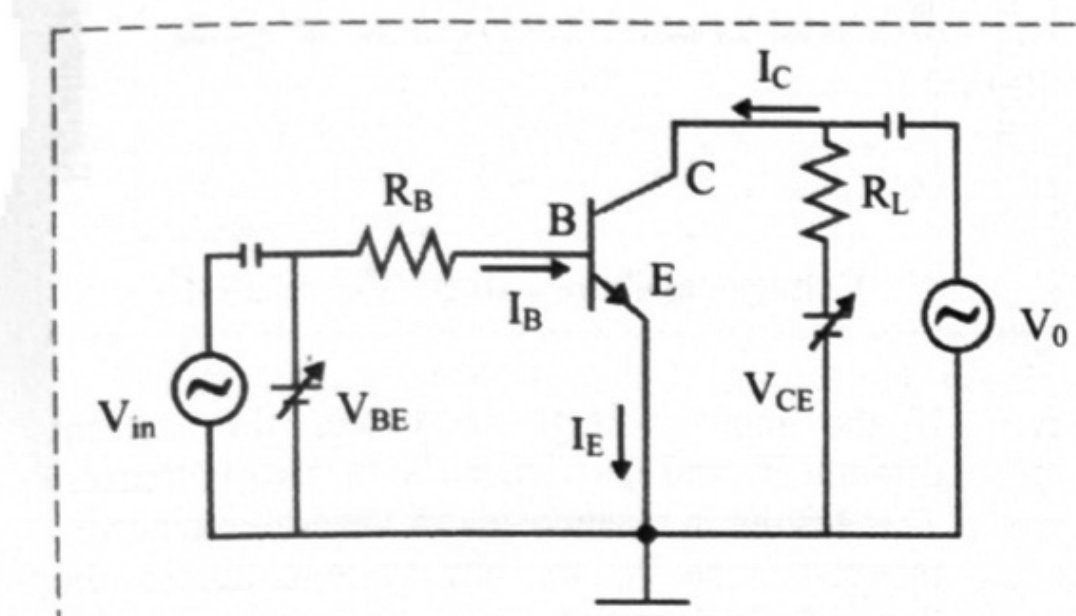
Circuit in words: the base is biased by a DC supply through a base resistance , and the small sinusoidal input signal is superimposed on this DC bias. The collector is supplied by through the load resistance . The output is taken across , through a capacitor connected in the output circuit to block the DC component so that only the amplified AC signal appears at the output.
Working
With no signal applied, Kirchhoff's law for the output loop gives
and for the input loop
When the AC signal voltage is applied at the input, the emitter-base voltage changes, so the emitter current changes and hence the collector current changes. The base current and the collector current carry the sinusoidal variation superimposed on their DC values.
Because is fixed, a change in forces a change in :
This change in the collector voltage is the amplified output of the input variation, and the negative sign shows that it is in antiphase with the input.
Gains
The AC current gain is defined as
and it is almost the same as at normal operating voltages. The output voltage is
The voltage gain is
The negative sign indicates that the output voltage and the input voltage are out of phase (by ). Since there is also a current gain in the common emitter configuration, the power gain is
taking the magnitude of . A transistor can give a power gain because .
An amplifier does not generate power. The additional power in the output comes from the DC supply ; the transistor only controls how much of that power reaches the load, following the small input signal.
Method of biasing used for operating a transistor as an amplifier: emitter-base junction forward biased and collector-base junction reverse biased.
Standard results
- ; of ; of ; . The largest current in a BJT is the emitter current.
- , , .
- , , typical between and .
- at constant ; at constant .
- ; ; ; .
- Barrier potential of a silicon transistor: to .
Worked numericals from the exercises
- Common base DC current gain , emitter current . , so .
- Emitter current , collector current . .
- Emitter current , collector current . .
Theory Questions Asked on This Subtopic
Real board questions. Answers are at the end of the page.
- 1
Draw neat labelled circuit diagram of a transistor used as common emitter amplifier. OR Draw a neat labelled circuit diagram for NPN transistor as an amplifier in a common emitter mode.
 Maharashtra HSC board question — asked in March 2008; March 2009Answer 1 ↓
 - 2
Draw a neat circuit diagram to study the characteristics of common emitter n-p-n transistor. With the help of a graph, explain the output characteristics of this transistor.
 Maharashtra HSC board question — asked in July 2017Answer 2 ↓
 - 3
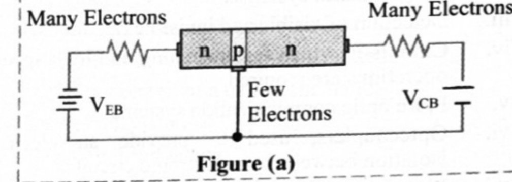
Explain the working of n-p-n transistor in common base configuration.
 Maharashtra HSC board question — asked in February 2023Answer 3 ↓
 - 4
What are and parameters for a transistor? Obtain a relation between them. OR Define and . Obtain the relation between them.
Maharashtra HSC board question — asked in February 2024; July 2022; March 2015Answer 4 ↓
Answers & Solutions
Work the questions above first, then check yourself here. Each answer is set out the way it should be written in the paper.
The question is a real board question. Its answer and working are ours — this paper was published without an official answer key.
Circuit: n-p-n transistor as a common emitter amplifier
The circuit is arranged as shown.
The connections, in words
- i. The emitter is the **common** terminal: it is earthed, and both the input and the output are measured with respect to it. Hence the name common emitter.
- ii. **Input (base) circuit.** The base is biased by the battery through the base resistance , so that the emitter-base junction is **forward biased**. The small alternating signal to be amplified is connected in series in this loop, superimposed on the d.c. bias.
- iii. **Output (collector) circuit.** The collector is fed from the supply through the load resistance , with the polarity chosen so that the collector-base junction is **reverse biased**.
- iv. The amplified output is taken between collector and emitter through the capacitor , which blocks the steady d.c. level and passes only the alternating part of the collector voltage.
Working, in brief
- v. With no signal applied, Kirchhoff's law gives for the input loop and for the output loop.
- vi. When is applied, changes, so changes, and the collector current changes times as much:
- vii. Since is fixed, this forces a change in the collector voltage,
which is the amplified output. The voltage gain is
Result
The circuit above is the common emitter amplifier: emitter-base junction forward biased, collector-base junction reverse biased, output taken across between collector and emitter, and out of phase with the input by .
Output characteristics: i. The variation of the collector current with variation in the collector-emitter voltage is called the output characteristic of a transistor. ii. While studying output characteristics of transistor, is kept constant. iii. From the curves of the output characteristics as shown in figure it can be observed that collector current is independent of as long as the collector-emitter junction is reverse biased. iv. Also, the collector current is large for large values of the base current when is constant.
Working of n-p-n transistor: i. Majority charge carriers in the emitter of n-p-n transistor are electrons. ii. A typical biasing of a transistor is shown in figure (a). In this, emitter-base junction is forward biased while collector-base junction is reverse biased. iii. At the instant when the EB junction is forward biased, electrons in the emitter region have not entered the base region as shown in figure (b). iv. When the biasing voltage is greater than the barrier potential (0.6 – 0.7 V for Si transistors), many electrons enter the base region and form the emitter current as shown in figure (c). v. These electrons can either flow through the base circuit and constitute the base current (), or they can also flow through the collector circuit and contribute towards the collector current (). vi. The base being thin and lightly doped, base current is only 5% of . vii. Electrons injected from the emitter into the base diffuse into the collector-base depletion region due to the thin base region. When the electrons enter the collector-base depletion region, they are pushed into the collector region by the electric field at the collector-base depletion region. The collector current () flows through the external circuit as shown in figure (d). The collector current is about 95% of . From the figure we can conclude that, Since the base current is very small we can write .
i. In case of common emitter configuration, is the ratio of the collector current to the emitter current. ii. Similarly, the current gain or the current amplification factor () is defined as the ratio of the collector current to the base current. iii. Since, Dividing throughout by , we have,